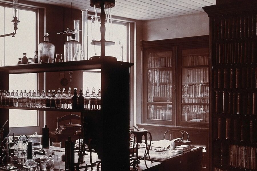
In university labs, hospitals, and maker spaces alike, microscopes are the everyday tools that let us see what’s otherwise invisible — from cell structures to nanomaterials. Knowing which instrument fits a task saves time and prevents frustration when planning experiments or buying equipment.
There are 32 Types of Microscopes, ranging from Atomic Force Microscope (AFM) to X-ray microscope (full-field). For each type, the data are organized with Magnification (×) / Resolution (nm),Common applications,Common locations so you can quickly compare capability, typical uses, and where you’re likely to find them; you’ll find below.
How do I choose the right microscope for my project?
Decide by sample type (biological, materials, surfaces), required resolution and magnification, whether you need live imaging or vacuum-compatible prep, and your budget; consider common locations listed below to match available facility equipment or services.
What causes the big resolution gap between light and electron microscopes?
The main limit is wavelength: visible light limits optical resolution to ~200 nm, while electrons have much shorter effective wavelengths, letting electron and scanning probe microscopes reach nanometer to sub-nanometer resolution, though they often need more complex sample preparation and environment control.
Types of Microscopes
| Name | Magnification (×) / Resolution (nm) | Common applications | Common locations |
|---|---|---|---|
| Simple microscope (magnifying glass) | 2–20× / ~100–500 µm | Quick visual checks, reading, coarse inspection | Home, fieldwork, classrooms |
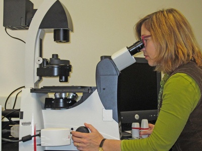
| Compound light microscope | 40–1,000× / ~200 nm | Cell biology, education, clinical slides | Schools, teaching labs, clinical labs |
| Stereo (dissection) microscope | 6–50× / ~10–50 µm | Dissection, specimen sorting, circuit board inspection | Field labs, workshops, biology labs |
| Inverted microscope | 40–1,000× / ~200 nm | Cell culture observation, live-cell imaging | Cell culture labs, incubators, research labs |
| Polarizing microscope | 40–1,000× / ~200 nm | Mineralogy, crystallography, polymer analysis | Geology labs, materials science labs, industry |
| Dark-field microscope | 40–1,000× / ~200 nm | Detecting small particles, live microbes, thin fibers | Clinical labs, environmental monitoring, research |
| Phase-contrast microscope | 40–1,000× / ~200 nm | Live-cell imaging, transparent samples, microbiology | Research labs, teaching labs, clinical labs |
| Differential Interference Contrast (DIC) microscope | 40–1,000× / ~200 nm | High-contrast cellular structures, live samples | Advanced research labs, imaging facilities |
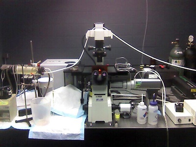
| Fluorescence (widefield) microscope | 40–1,000× / ~200 nm | Protein localization, cellular markers, diagnostics | Biology labs, pathology labs, research centers |
| Confocal laser scanning microscope | 40–1,000× / ≈200 nm lateral | 3D imaging, thick tissue stacks, colocalization studies | Core facilities, advanced research labs, imaging centers |
| Two-photon (multiphoton) microscope | 10–40× / ≈300 nm lateral, ≈1,000 nm axial | Deep tissue imaging, live animal studies | Neuroscience labs, in vivo imaging centers |
| Total Internal Reflection Fluorescence (TIRF) microscope | 40–100× / ≈200 nm lateral, ≈100 nm axial | Membrane studies, single-molecule events, cell adhesion | Cell biology labs, biophysics labs |
| Light-sheet fluorescence microscope (LSFM / SPIM) | 10–40× / ≈200 nm lateral, 500–1,000 nm axial | Fast 3D imaging, developmental biology, cleared tissue | Imaging cores, developmental biology labs |
| Structured Illumination Microscope (SIM) | 40–1,000× / ~100 nm | Enhanced resolution fluorescence imaging, live-cell super-resolution | Advanced imaging facilities, research labs |
| Stimulated Emission Depletion (STED) microscope | 40–1,000× / ~20–50 nm | Super-resolution imaging of proteins and organelles | Specialized imaging centers, research institutes |
| PALM/STORM (single-molecule localization) | 40–1,000× / ~10–20 nm | Molecular-scale localization, nanoscale architecture | High-end research labs, super-resolution centers |
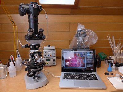
| Digital holographic microscope | 10–200× / ~200 nm | Phase imaging, cell counting, dynamic studies | Industry labs, research groups, quality control |
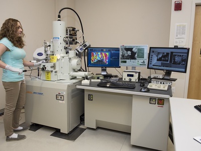
| Scanning Electron Microscope (SEM) | 20–1,000,000× / ~1–20 nm | Surface topography, materials, failure analysis | Materials labs, industry, research centers |
| Environmental SEM (ESEM) | 20–500,000× / ~5–30 nm | Wet samples, biological specimens, powders | Research labs, microscopy facilities |
| Transmission Electron Microscope (TEM) | 50,000–10,000,000× / ~0.05–0.2 nm | Ultrastructure, viruses, nanomaterials | Research institutes, EM cores, materials labs |
| Cryo-Electron Microscopy (cryo-EM) | 50,000–1,000,000× / ~0.3 nm | Macromolecular structures, structural biology | Structural biology labs, cryo-EM facilities |
| Scanning Transmission Electron Microscope (STEM) | 50,000–10,000,000× / ~0.1–0.2 nm | Atomic-scale imaging, spectroscopy, materials analysis | Advanced EM facilities, materials science labs |
| Helium Ion Microscope (HIM) | 1,000–1,000,000× / ~0.5–1 nm | High-resolution surface imaging, nanofabrication | Nanotech labs, advanced imaging centers |
| Focused Ion Beam–Scanning Electron Microscope (FIB-SEM) | 20–500,000× / ~1–5 nm | 3D tomography, site-specific milling, failure analysis | Microfabrication labs, materials labs, research facilities |
| Atomic Force Microscope (AFM) | N/A / ~0.1 nm vertical; ~1 nm lateral | Surface topography, force measurements, nanoscale manipulation | Nanotech labs, materials science, industry |
| Scanning Tunneling Microscope (STM) | N/A / ~0.1 nm | Atomic-scale surface structure, electronic states | Surface science labs, condensed-matter research |
| Scanning Near-field Optical Microscope (SNOM/NSOM) | N/A / ~10–100 nm | Optical imaging beyond diffraction, nano-optics | Optics labs, nano-imaging facilities |
| Magnetic Force Microscope (MFM) | N/A / ~10–50 nm | Magnetic domain imaging, data storage research | Materials labs, magnetic device research |
| X-ray microscope (full-field) | N/A / ~30 nm | High-resolution internal imaging, materials, biology | Synchrotrons, specialized imaging centers |
| X-ray micro-CT (micro-computed tomography) | N/A / ~1–50 µm | 3D internal structure, fossils, engineering parts | Industrial labs, paleontology, materials testing |
| Raman microscope | 40–1,000× / ~200 nm optical; chemical mapping ~500 nm–1 µm | Chemical identification, material mapping, pharmaceuticals | Chemistry labs, materials labs, industry |
| FTIR / Infrared microscope | N/A / ~3–10 µm | Chemical imaging, polymer analysis, pharmaceuticals | Analytical labs, materials labs, industry |
Images and Descriptions

Simple microscope (magnifying glass)
A single-lens instrument that magnifies small objects for casual inspection. It’s cheap, portable and easy to use but limited in detail—good for hobbyists, outdoor work, and quick visual checks when microscopy-grade resolution isn’t needed.
Compound light microscope
A standard multi-lens optical microscope using transmitted light to view thin, stained samples. It balances magnification and resolution for routine biology and medical work, making it the go-to tool in classrooms and diagnostic labs.
Stereo (dissection) microscope
Binocular, low-magnification microscope that gives a 3D view of surfaces and larger specimens. It’s ideal for dissection, assembly work, and quality control where depth perception and hands-on manipulation matter.
Inverted microscope
A compound microscope with objectives beneath the stage to view samples from below—perfect for observing cells in dishes or flasks. Its design suits live-cell imaging and experiments requiring easy access to the specimen.
Polarizing microscope
Uses polarized light to reveal birefringence and crystal structure in samples. Essential for identifying minerals, fibers, and stresses in materials; it highlights features invisible under standard brightfield illumination.
Dark-field microscope
Dark-field illumination makes tiny or translucent objects glow against a dark background, improving visibility of bacteria, particulates, and delicate structures that are hard to see in brightfield.

Phase-contrast microscope
Enhances contrast in unstained, transparent specimens by converting phase shifts into intensity differences. Phase contrast is widely used for observing living cells, motility, and thin biological samples without dyes.
Differential Interference Contrast (DIC) microscope
DIC gives high-contrast, pseudo-3D images of transparent specimens by using interference. It’s prized in cell biology for revealing fine structure and edges without staining, producing a shadowed, detailed look.
Fluorescence (widefield) microscope
Excites fluorescent dyes or proteins and collects emitted light to visualize specific molecules. Widefield fluorescence is versatile and common for locating labeled structures, though out-of-focus light can reduce clarity in thick samples.
Confocal laser scanning microscope
Uses focused lasers and pinholes to block out-of-focus light, producing sharp optical sections and 3D reconstructions. Confocal is ideal for detailed imaging inside tissues and co-localization of fluorescent markers.
Two-photon (multiphoton) microscope
Excites fluorescence with near-infrared light via simultaneous photon absorption, allowing deeper imaging with less photodamage. It’s the preferred method for live tissue and small-animal imaging at depth.
Total Internal Reflection Fluorescence (TIRF) microscope
Illuminates only a thin region near a coverslip surface using an evanescent wave, providing very high axial contrast. Great for studying events at the cell membrane or single-molecule surface interactions.
Light-sheet fluorescence microscope (LSFM / SPIM)
Illuminates specimens with a thin sheet of light from the side for gentle, fast volumetric imaging. It’s excellent for long-term live imaging and large, cleared samples with reduced photobleaching.
Structured Illumination Microscope (SIM)
SIM uses patterned light and computational reconstruction to roughly double resolution over diffraction limits while remaining relatively fast and compatible with live samples—useful for higher-resolution fluorescence studies.
Stimulated Emission Depletion (STED) microscope
A super-resolution method that shrinks the effective fluorescent spot using a depletion beam, giving tens-of-nanometers resolution. STED enables detailed structural studies below the diffraction limit but requires specialized dyes and optics.
PALM/STORM (single-molecule localization)
Single-molecule localization techniques switch fluorophores on and off, localizing them with high precision to build super-resolved images. They achieve molecular-scale resolution for dense protein mapping but need careful sample prep.
Digital holographic microscope
Captures holograms and reconstructs amplitude and phase images computationally to measure shape and motion without staining. It’s noninvasive and fast, useful for live-cell dynamics and quantitative morphology measurements.
Scanning Electron Microscope (SEM)
Scans a focused electron beam across surfaces to render high-depth-of-field, high-resolution images of topography and composition contrasts. SEMs are staples in materials science and microscopy cores for detailed surface inspection.
Environmental SEM (ESEM)
An SEM variant that allows imaging at higher pressures and with hydrated samples, reducing the need for extensive drying or coating. ESEM is useful for biological specimens and volatile materials that would be damaged in standard SEMs.
Transmission Electron Microscope (TEM)
Transmits electrons through ultrathin samples to reveal internal structure at near-atomic resolution. TEM is essential for cell ultrastructure, crystallography, and nanoscience but requires demanding sample preparation.
Cryo-Electron Microscopy (cryo-EM)
Samples are flash-frozen and imaged in vitreous ice to preserve native structure, allowing near-atomic reconstructions of proteins and complexes without staining or crystals—transformative for modern structural biology.
Scanning Transmission Electron Microscope (STEM)
Combines scanning beam control with transmitted electron detection for high-resolution imaging and elemental analysis. STEM excels at correlating structure and composition down to the atomic scale.
Helium Ion Microscope (HIM)
Uses helium ions instead of electrons to produce images with high surface sensitivity and contrast, excellent for fine surface details and nanofabrication tasks where SEM contrast is limited.
Focused Ion Beam–Scanning Electron Microscope (FIB-SEM)
Combines focused ion milling with SEM imaging to cut and image materials slice-by-slice, enabling 3D reconstructions and precise sample preparation for TEM or analysis.
Atomic Force Microscope (AFM)
A scanning probe that uses a sharp tip to map surface forces and topography with sub-nanometer vertical resolution. AFM works in air or liquid and measures mechanical properties at the nanoscale.
Scanning Tunneling Microscope (STM)
Measures tunneling current between a conductive tip and sample to image and manipulate individual atoms and electronic states on conductive surfaces with atomic resolution.
Scanning Near-field Optical Microscope (SNOM/NSOM)
Combines a sharp, near-field probe with optical detection to beat the diffraction limit, providing optical contrast at tens of nanometers—useful for photonic structures and nanoscale light mapping.
Magnetic Force Microscope (MFM)
A derivative of AFM that senses magnetic forces between a magnetized tip and sample to map magnetic domains and structures at the nanoscale, important for memory and spintronics research.
X-ray microscope (full-field)
Uses X-rays to image internal structure with higher penetration than visible light and finer resolution than lab X-ray sources. It’s valuable for non-destructive internal imaging of materials and biological samples.
X-ray micro-CT (micro-computed tomography)
Rotating X-ray tomography that produces 3D volumes revealing internal features without sectioning. Micro-CT is widely used for inspection, biological anatomy, and materials porosity analysis.
Raman microscope
Combines microscopy with Raman spectroscopy to provide spatially resolved chemical information. It’s non-destructive and useful for identifying compounds, mapping compositions, and studying materials in situ.
FTIR / Infrared microscope
Uses mid-infrared absorption to map chemical bonds and functional groups with micron-scale resolution. FTIR microscopy is valuable for materials characterization and identifying chemical heterogeneity in samples.